NanoSat-1B
Non-EO
INTA
Quick facts
Overview
| Mission type | Non-EO |
| Agency | INTA |
| Launch date | 29 Jul 2009 |
NanoSat-1B
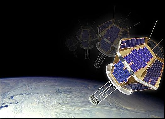
NanoSat-1B is a follow-up small microsatellite technology demonstration mission of NanoSat-1 (launch Dec. 18, 2004) of INTA (Instituto Nacional de Tecnica Aerospacial), the Spanish Space Agency, Madrid., Spain.
Spacecraft
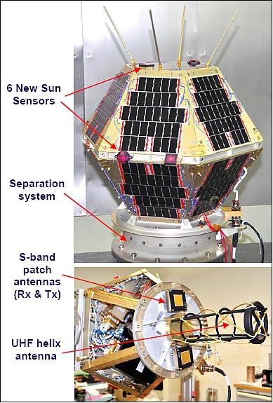
ACS (Attitude Control Subsystem): NanoSat-1B is inheriting the new 3-axis magnetic sensor design of NanoSat-1, using a commercially available AMR (AnisotropicMagnetoresistive) device from Honeywell (HMC1921S). Based on the good results in orbit (robustness, accuracy & low power consumption), the same design is ready to fly in the NanoSat-1B spacecraft (and was selected for INTAµSat-1). NanoSat-1B is Earth pointing. 1) 2) 3)
The attitude is being sensed with CSS (Coarse Solar Sensors) taking advantage of the two different designs flying on NanoSat-1 (2 sets with 3 space qualified GaAs, together with 2 more nanosensors with 3 experimental porous Si cells each) which are still running in orbit after 4.5 years in 2009. A small design change was introduced with GaAs cells that provide 0.2º accuracy in a quasi hemispherical angular aperture.
Three experimental micro-sensors, called VectorSol, are being introduced into the ACS. They have been developed by UPC (Universidad Politecnica de Barcelona) together with the US (University of Sevilla), and qualified at INTA facilities. VectorSol is a 4-cell µsun sensor (30 mm x 50 mm & 0,1º in 120º FOV) along with a PIC microprocessor and its flight software.
EPS (Electrical Power Subsystem): A new Li-ion battery assembly from SAFT is being used 2 x (5.8 Ah capacity, 24 V).
OBDH (On Board Data Handling) subsystem: A Mil-883 68332 processor is being used, previously tested for radiation tolerance, together with a latch-up protection circuit that avoids destruction in case of a latch-up build-up.
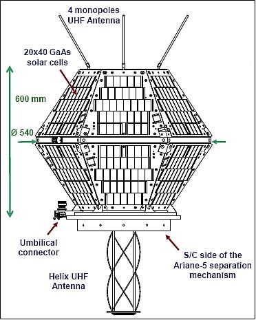
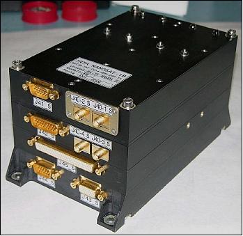
NanoSatellite-1B spacecraft has a mass of 23.9 kg, the expected lifetime is 5 years.
Mission | Store & Forward in UHF band (400 MHz) up to 40 kbit/s bidirectional, including mobile users service |
R&D payload | Proton detector (LDT), Experimental Magnetic Sensor (MI), RadFET, 3 Fine Solar Sensors with 0.2º |
Lifetime | Target of 3 years, extended mission of 5-7 years, possibly > 10 years |
Orbit | SSO, altitude of 677 km x 586 km, inclination =98.09º, LTAN=11 hours, period=97.34 minutes |
Spacecraft size | 44 cm between sides and 47 cm body height |
Spacecraft mass | 23.9 kg with 7075 Aluminum structure |
EPS | Panels: 13 of 32 GaAs/Ge cells with 23 W of power |
OHDH | Motorola 68332 microprocessor with 512 kB EEPROM & 2 MB RAM |
ACS | Zero momentum 3-axis stabilized control with nadir pointing (5º) using 3 magnetorquer coils, 3 solar sensors (±90º each) and 1 triaxial magnetic sensor with 4 AMRs |
RF communications | TM: 4.5 W RF, 40 kbit/s TM at 387.1 MHz; TC at 400 MHz. S-band TM-TC at 2.043 & 2.223 GHz 40-175 kbit/s |
Launch
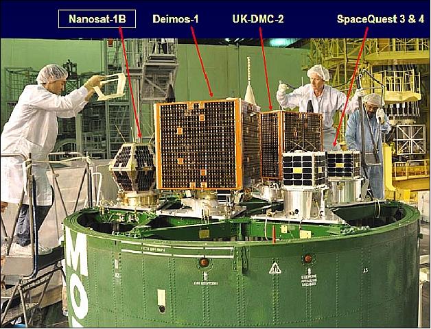
NanoSat-1B was launched as a secondary payload on July 29, 2009. The launch site was Baikonur, Kazakhstan. The launch provider was ISC (International Space Company) Kosmotras of Moscow, Russia (Dnepr vehicle).
The shared payload manifest of the launch was:
• DubaiSat-1 an imaging minisatellite of the UEA (United Arab Emirates) Institution for Advanced Science and Technology (EIAST) is the main payload on this flight (mass of ~ 190 kg)
• Deimos-1 (Spain), UK-DMC-2 (United Kingdom), each with a mass of ~ 96 kg
• AprizeSat-3, AprizeSat-4, LEO communication experiments of Aprize Satellite Inc., Fairfax, VA, USA (built by SpaceQuest Ltd., each with a mass of 12 kg)
• NanoSat-1B of INTA (Instituto Nacional de Técnica Aeroespacial), Spain (23.5 kg).
Orbit: Sun-synchronous near-circular orbit, altitude 578 km x 706 km, inclination = 98.1º, the orbital period is about 97.3 minutes, the LTAN (Local Time on Ascending Node) is at 10:30 hours.
RF communications: A new S-band transceiver is being intoduced for TT&C service provision. The instrument has a size of 106 mm x 166 mm x 90 mm and a mass of 1.6 kg, providing a downlink rate capability of up to 2 Mbit/s and an uplink of 100 kbit/s. - However, for NanoSat-1B, lower data rates (100-200) kbit/s, depending of the selected FEC by TC (1/2 to 7/8) are being used, to be able to test the new FPGA design (Ref. 1).
Only a small 2.5 m dish antenna is being used at the control center in Madrid - which limits the use of the full downlink capacity.
In addition, a VHF/UHF uplink and downlink is installed for reasons of redundancy.
Mission Status
• The NanoSat-1B spacecraft and its sensor complement are operating nominally in 2012. 5)
- INTA developed small “nano-terminals” for the ground segment. These are portable user stations, of small suitcase size, that allow communication with the satellite. The mobile stations are intended to provide store&forward communications in remote regions (Ref. 5).
Sensor Complement
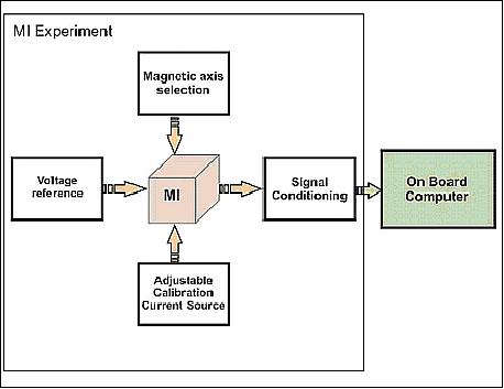
MI/RadFET (Magneto-Impedance/Radiation-sensitive Field Effect Transistor)
The Mi/RadFET is an in-orbit validation experiment of a new technology of magnetic sensors. The project selected the AMI-302 (Aichi Steel Corporation) device, a COTS 3-axis magnetic sensor based on magneto-impedance that integrates some conditioning electronics front-end, manufactured in a CMOS process.
The AMI-302 is operated from a high-stability 3 V reference. The IC itself integrates the pre-conditioning electronics for the 3 orthogonal magnetic sensors inside, as well as multiplexing. Two digital signals allow for the selection of the axis to be read. Further conditioning electronics is added for post-amplification and filtering, before delivering the signal to an A/D converter in the OBDH (On Board Data Handling) signal acquisition chain.
To calibrate the sensor, a current varying among several fixed values is applied to a coil that generates a constant magnetic field for the three axes -prior to each measurement. - There is also a small temperature sensor (PT-1000) mounted to the body of the AMI, which allows temperature monitoring.
Several TID (Total Ionizing Dose) sensitive devices (RadFETs) were added to obtain a better knowledge of the total ionizing dose received at the MI PCB (Printed Circuit Board). Two different RadFET chips (Tyndall National Institute) are used: one with a gate-oxide thickness of 400 nm, the other with 1 µm thickness. It should be noted that, while 400 nm RadFETs are the most standard Tyndall part used in space missions, this is the first flight of the more sensitive 1 µm RadFET part.
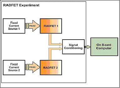
The idle state of the RadFET module is the irradiation mode, during which the RadFETs accumulate dose. In this mode, all RadFET terminals (bulk, source, gate, and drain) are grounded; the RadFET is in an off-state.
The read-out mode is activated by means of a ground telecommand. The command causes the activation of two digital signals, each of them controlling the activation of a separate current source. The current source is applied to the RadFET source terminal which in this configuration is tied to the bulk. The shift in this voltage, also known as threshold voltage (VT) is representative of TID. This voltage is conditioned and adapted to the OBC requirements. The current value is also sensed for reference.
LDT (Las Dos Torres)
LDT (The Two Towers- in Spanish) is a proton monitor onboard NanoSat-1B. The radiation monitoring instrument measures the effect of protons (i.e., displacement damage) on two kinds of optoelectronic components: photodiodes and LEDs (Light Emitting Diodes). 6)
Working principle: In the LDT, the increase of the photodiodes dark current and the decrease of the LEDs emissivity are used to calculate the radiation induced by protons. To select the most adequate devices, several features were taken into account. For example, their size and package must be suitable for space missions and they must have a sufficiently high sensitivity to proton radiation. These devices have been irradiated by INTA several times to analyze their degradation under proton irradiation.
The flight model unit was calibrated in order to know the actual sensitivity of the sensor samples that are encountered in flight.
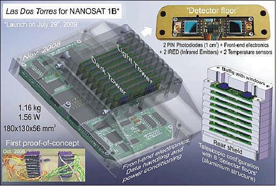
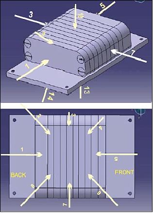
The instrument has a mass of 1.6 kg and a power consumption of 1.56 W (from 12 V, -12 V and 5 V). Its dimensions are 180 mm length, 130 mm width, and a maximum height of 56 mm. All sensing elements are aligned along an axis and housed inside an aluminum structure, with eight detecting floors in a telescopic configuration, a front window and a rear shield. The sensing elements are functionally grouped into two stacks: the ‘dark’ and ‘light’ towers (Figure 8).
There are two different ways of measuring the radiation with the LDT photodiodes. The first one is to obtain the proton fluence through the displacement damage effects. The second one is to measure the ionizing current, which is proportional to the received proton flux.
Since the sensors in the LDT are shielded with aluminum foils of different thicknesses, the minimum proton energy that can be detected at each floor is different. In this way, spectral information of the radiation environment can be obtained.
The fluence and flux results of protons above 75 MeV that are detected by the LDT in the NanaSat- 1B satellite can be derived. Moreover, the percentage flux variations of the 8 different energy channels can also be obtained.
Shielding: The minimum proton energy needed to reach the sensors depends on the shielding. Two different threshold energies are used in this work: the theoretical one and the empirical one. Threshold energies are defined here as the minimum energy that a proton must have in order to reach a sensor with a probability of 80%.
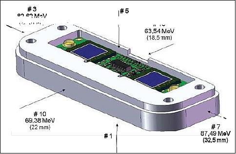
Legend to Figure 9: Directions # 1 and #5 are at right angles to the sensors from the front side and the back one, respectively. Due to the global structure, the equivalent shielding and the threshold energies are different for each floor in these two directions.
The actual shielding at each floor has been studied. In this study, it is demonstrated that the 7th floor provides data on the protons above ~75 MeV that reached the instrument from all directions. For this purpose, the directions depicted in Figure 9 and Figure 10, were taken into account. For each direction, both the theoretical threshold energy and the empirical one were obtained.
Each LDT floor has different equivalent shieldings, depending on the angle of incidence. At right angles to the sensors, the shielding is different for each floor in both the front direction (direction #5) and the back one (direction #1). On the other hand, the shielding in the rest of directions is, in first approximation, the same for all the floors.
Results (Ref. 6): Between January 2010 and March 2011, the LDT was activated every 2 minutes, that is, 216 times a day: 108 times between 1:00 and 4:18 (UTC), and another 108 times between 13:00 and 16:18 (UTC). Thus, the LDT is being activated for more than 2 orbits in the early morning and in the afternoon. Thus, ~ 4 complete orbits over the western part of the South Atlantic Anomaly (SAA) region and obviously 4 passes over each pole.
Since March 2011 the activations have taken place between 21:00 and 4:18 (UTC) and 9:00 and 16:18 (UTC), every 2 minutes. In other words, there have been 438 activations a day and ~9 complete orbits in the SAA region and poles.
In a first stage after the launch of the spacecraft, from August 3, 2009 until 2010, data was also collected but not in the aforementioned periodical manner. It must be pointed out that sometimes the experiment could not be activated due to housekeeping tasks in the satellite. To sum up, the data presented was taken during 518 days, from August 4, 2009 to August 22, 2011.
NanoSat-1B visits the same geographical position, i.e. the same latitude and longitude, every 4 days. However, it takes about 3 months to be at the same altitude (but the exact period depends on the altitude). Due to the type of orbit, data is collected for altitudes between ~588 km and ~706 km.
VectorSol
VectorSol is a new MEMS sun sensor design program to be introduced on the NanoSat-1B spacecraft as a technology validation for use in future pico- and nanosatellite missions. Important properties of such sun sensors are the FOV (Field of View), the pointing accuracy (mrad), the data format (analog or digital), and the size and mass of the device. 7) 8)
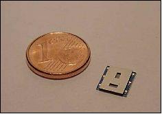
The new MEMS device, designed and manufactured by INTA, is a 2-axis analog sun sensor. The sensor is made of four silicon photodiodes monolithically integrated in a crystalline silicon substrate, protected by a transparent cover glass assembled on the same silicon die against space radiation damage. The sensor fabrication combines standard silicon processing technology with a high performance solar cell fabrication process. The sensor, including electronics and mechanical and electrical interfacing with the satellite, has a small size (3 cm x 3 cm) and low mass (24 gram), with a sun FOV field-of-view greater than ±60º with an angle accuracy better than 0.15º. Three of these sensors have been integrated in the NanoSat-1B platform.
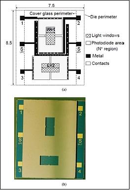
Legend to Figure 11: All dimensions are in mm. In a) the contour in the dashed line indicates where the cover glass will be placed onto the silicon die. In b) the emitter or cathode electrodes (pads labeled 1–4) and base or anode electrodes (two redundant electrodes labeled S “Substrate”) are easily distinguished in the image. At the center of the each window, four small features can be seen to perform the fine alignment between the cover glass and the silicon substrate.
The total silicon die area (Figure 11) is 0.75 cm 0.85 cm. The cover glass has a smaller width than the silicon substrate to allow the wire-bonding in the periphery. The electrode pads were also used to pre-align the cover glass to the silicon die. The window placement and the distance between the photodiode pairs were calculated to avoid light coupling between them in the whole angle range of measurement.
The fabrication of the silicon device has been done in the Laboratory of the MNT (Micro & Nano Technology) group of the UPC. The sensor fabrication combines standard processes used in silicon technology, with processing currently used at the MNT group to build high performance photovoltaic devices and solar cells. The device fabrication sequence has three main stages: silicon die fabrication, cover glass metallization defining the two light windows, and cover glass bonding to the silicon die.
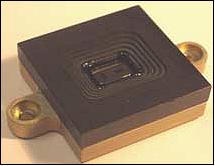
Sensor calibration has been performed at the Laboratory of Certification of photovoltaic solar cells for space use, SPASOLAB, located at INTA.
The sun sensors manufactured fulfill the mission requirements yielding a sun FOV of ±60º with an angle accuracy better than 0.15º.
References
1) Manuel Angulo, Laura Seoane, Elisa Molina, Manuel Prieto, Oscar Rodriguez, S.egundo Esteban, Jordi Palau, Stefania Cornara, “INTAµSat-1 First Earth Observation Mission,” Proceedings of the 7th IAA Symposium on Small Satellites for Earth Observation, Berlin, Germany, May 4-7, 2009, IAA-B7-0202, URL: http://media.dlr.de:8080/erez4/erez?cmd=get&src=os/IAA/archiv7/Presentations/0202_ANGULO%20IAA-B7-0202.pdf
2) M. F. Cerdán, A. B. Fernández, J. J. Jiménez, M. D. Michelena, “Witnessing variations in the Earth magnetic field by means of NanoSat-1B COTS AMR magnetic sensor,” Geophysical Research Abstracts, Vol. 13, EGU2011-6768-2, 2011, URL: http://meetingorganizer.copernicus.org/EGU2011/EGU2011-6768-2.pdf
3) M. F. Cerdán, M. D. Michelena, “In orbit calibration of COTS AMR magnetic sensor,” Geophysical Research Abstracts, Vol. 13, EGU2011-6330-1, 2011, URL: http://meetingorganizer.copernicus.org/EGU2011/EGU2011-6330-1.pdf
4) Manuel Angulo, Laura Seoane, Jorge Rivas, Alejandro Gimeno, Manuel Pietro, Oscar Rodriguez, Segundo Esteban, “The second generation NanoSat-2 program at INTA,” Proceedings of the 8th IAA Symposium on Small Satellites for Earth Observation, April 4 – 8, 2011, Berlin, Germany, paper: IAA-B8-0103
5) Information with regard to the mission status and the entire documentation of the sensor complement was provided by Ignacio Arruego Rodriguez of INTA, Madrid, Spain.
6) J. J. Jiménez, J. M. Oter, V. Apéstigue, C. Hernando, S. Ibarmia, W. Hajdas, J. Sanchez-Páramo, M. T. Álvarez, I. Arruego, H. Guerrero, “Proton monitor Las Dos Torres: first intercomparison of in-orbit results,” Proceedings of RADECS 2011 (Conference on Radiation Effects on Components and Systems), Sevilla, Spain, Sept. 19-23, 2011
7) J. Garcia Ortega, C. L. Tarrida, J. M. Querol, F. J. Delgado, P. Ortega, L. Castanier, M. Reina, M. Angulo, Y. Morilla, J. Garcia Lopez, “MEMS solar sensor testing for satellite applications,” Proceedings of the 2009 Spanish Conference on Electron Devices, Feb 11-13, 2009, Santiago de Compostela, Spain
8) Pablo Ortega, Gema López-Rodríguez, Jordi Ricart, Manuel Domínguez, Luis M. Castañer, José M. Quero, Cristina L. Tarrida, Juan García, Manuel Reina, Ana Gras, Manuel Angulo, “A Miniaturized Two Axis Sun Sensor for Attitude Control of Nano-Satellites,” IEEE Sensors Journal, Vol. 10, No 10, October 2010, pp. 1623-1632
The information compiled and edited in this article was provided by Herbert J. Kramer from his documentation of: ”Observation of the Earth and Its Environment: Survey of Missions and Sensors” (Springer Verlag) as well as many other sources after the publication of the 4th edition in 2002. - Comments and corrections to this article are always welcome for further updates (eoportal@symbios.space).