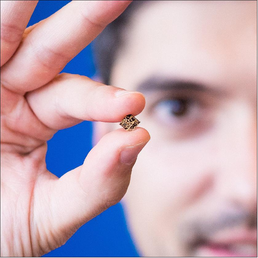
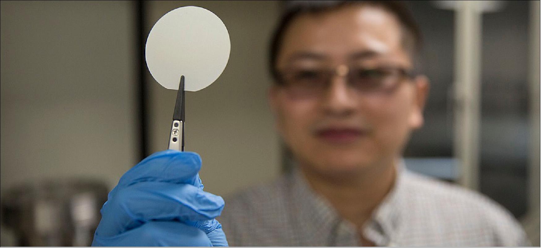
GaN-Chips (Gallium Nitrite Chips)
Tools and Platforms
GaN (Gallium Nitrite) Chips - Powering Space Missions
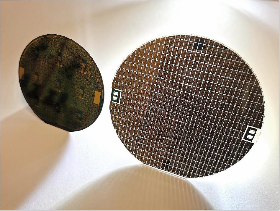
Some of ESA’s most ambitious future missions for telecommunications and Earth observation have only become possible because of a switch to a novel high-power and high-temperature capable semiconductor – sometimes termed the most promising material since silicon. ESA laboratory testing has confirmed the performance of key European-made Gallium Nitride components. 1)
Without knowing it, you already own some Gallium Nitride (GaN) crystals. GaN-based Light Emitting Diodes generate the laser light used to play Blu-Ray discs, provide backlight for modern TV and computer screens and sit within high-efficiency LED light bulbs. The latest slimline chargers for laptop batteries also incorporate GaN-based power converters.
As a ‘wide bandgap’ semiconductor, GaN can operate at much higher voltages and temperatures than traditional materials such as silicon or gallium arsenide. It was first commercially employed in the 1990s as an energy-efficient method of generating blue light.
Today – as silicon-based power devices move towards the limit of their operating temperature, breakdown voltage and power density – GaN is increasingly favoured for Radio Frequency (RF) signal amplification as well as very high power switching systems.
ESA’s ESTEC technology centre in the Netherlands recently oversaw lifetime testing of GaN-based high-power amplifier monolithic microwave integrated circuits (MMICs), the basis of a Dual Solid State Power Amplifier design being developed by SENER in Spain through ESA’s PACIS3 Partnership Project, set to operate aboard a pair of next generation Hisdesat telecom satellites, due to launch in 2023-4.
“These integrated circuits rely on a state of the art 0.25 μm gate length GaN technology from United Monolithic Semiconductors,” comments ESA engineer Václav Valenta who supports various developments of active antenna payloads. “This means the transistor gate terminals are fabricated onto the Gallium Nitride semiconductor chips to a size of 0.25 µm.
“Our lifetime-test results demonstrate excellent performance of the selected GaN process. This is good news, since the X-band multibeam active antenna payload under development for these satellites will rely on hundreds of such active GaN elements.”
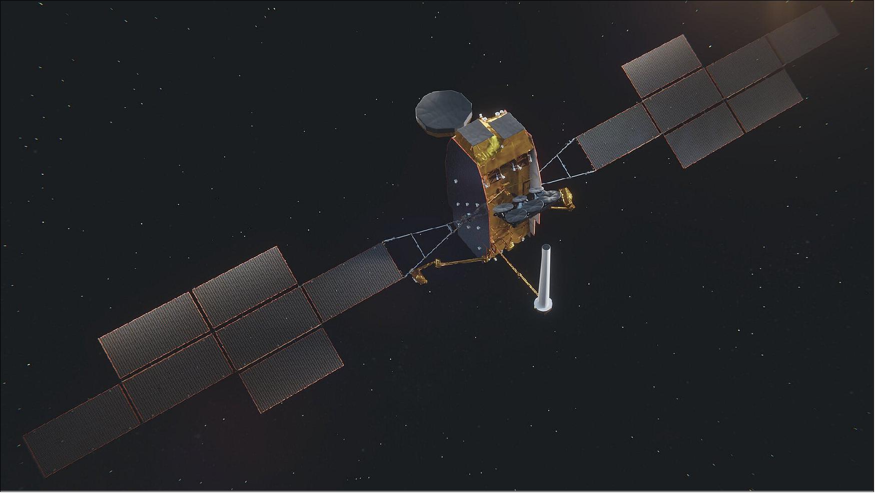
As well as being indispensable to these new telecom missions, GaN technology also sits at the heart of ESA’s ambitious Biomass satellite. Due to be launched next year, Biomass will deploy a massive 12-m diameter reflector to harness long-wavelength ‘P-band’ radar signals, piercing through forest canopies in order to perform a five-year census of all the trees on Earth. The mission as designed is only made possible by GaN-based RF amplifiers, boosting the transmitted RF signals that are then reflected by Earth’s forests back to the satellite.
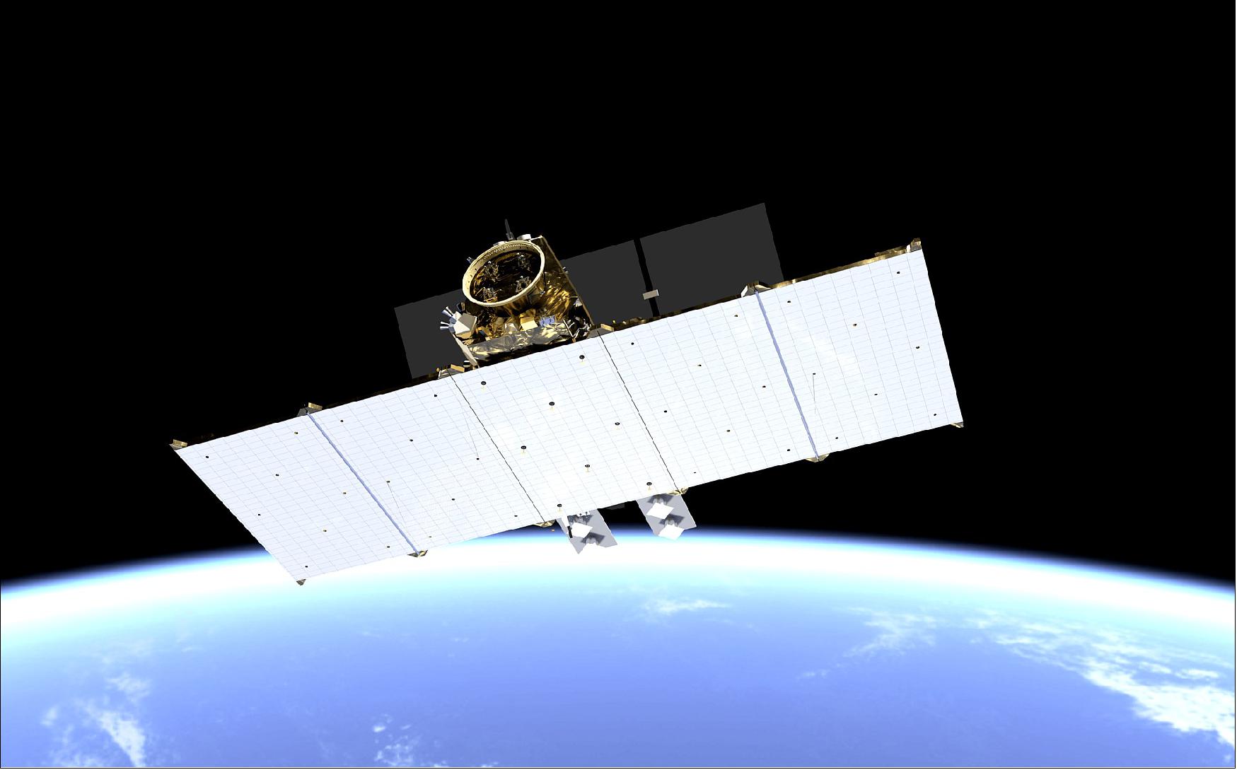
Looking further ahead, GaN technology will also serve the planned next generation of Copernicus Sentinel-1 radar satellites, with the potential to reduce the overall size of the spacecraft’s C-band transmit-receive modules while boosting its performance and scientific return.
Another forthcoming radar satellite, the high-resolution imaging ROSE-L (Radar Observation System for Europe in L-band), will incorporate the highest RF power solid-state transmit-receive modules ever flown in space, thanks to GaN transistors supplying nearly 200 W of power at L-band frequencies. Its active phased array synthetic aperture radar antenna will be the largest planar antenna ever built, measuring an impressive 11 metres by 3.6 metres – roughly the size of 10 ping-pong tables.
“Demonstration and testing is really key to greater adoption of GaN, despite its clear advantages,” adds Václav. “Mission managers tend towards tried and tested technology choices because they desire reliability above all. So rigorous assessment and testing of GaN technology on the ground is essential to understand its potential and limitations, and find solutions making the technology space-compliant in terms of reliability margins. This is what will eventually lead to the mainstream use of GaN technology in space.”
Preparing GaN for Space
ESA identified the promise of GaN early. In 2008 the Agency initiated its GaN Reliability Enhancement and Technology Transfer Initiative (GREAT2), bringing together leading research institutes and manufacturing industry to set up an independent European supply chain to manufacture high-quality GaN devices for space applications.
“We could see that Gallium Nitride had the potential to revolutionise communications in space, leading to a five- to ten-fold signal strength and data transmission rates” explains ESA’s Andrew Barnes, overseeing GREAT2.
“GaN-based systems also require much less in the way of active cooling, and have a reliability rate that can be measured in decades. As an added inducement for the space sector, they are also inherently radiation resistant. What GREAT2 proceeded to do was establish the performance and reliability of European GaN supply chains, including the flight of the very first GaN-based hardware in space, aboard PROBA-V in 2013.”
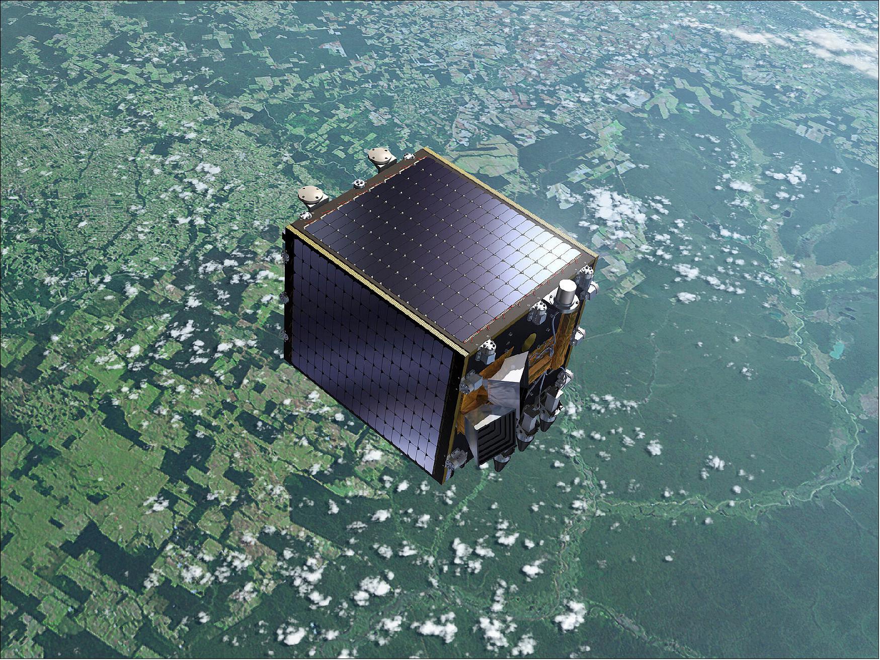
Earth-observing PROBA-V included a GaN amplifier in its X-band communication system, used to downlink images to Earth, which operated faultlessly for more than seven years until the satellite completed its final operations.
Andrew concludes: “The progress made by ESA in the development of GaN technology over the last decade has been paying off and this is demonstrated by multiple examples where GaN is adopted as baseline for critical RF payloads.
“While the mainstream GaN processes used in ESA’s missions are fully qualified or are in the process of obtaining qualification labels, ESA is also investing in development of new advanced GaN technologies for space, working together with the key industrial partners and research centres in Europe to further improve the performance, reach higher frequencies for next generation mm-wave payloads and assure a reliable end-to-end supply chain.”
UMS and OMMIC are the two European commercial sources for advanced GaN and also Gallium Arsenide integrated circuits and qualified semiconductor processes, as specified in ESA’s European Preferred Part list (EPPL).
EEE Space Component Sovereignty for Europe
Can a space mission really be described as European if a majority of its component parts comes from beyond our borders? ESA is proposing the EEE Space Component Sovereignty for Europe initiative for approval by Europe’s space ministers at the Agency’s Council at Ministerial Level at the end of 2022.
Working with industry and key partners, the initiative will reduce the dependence of Europe's space sector on non-European component suppliers, focusing on one of the building blocks of space missions - Electrical, Electronic and Electromechanical (EEE) components. A key aim shall be to develop state-of-art mm-wave GaN processes in Europe.
Development Status of GaN Technology
• February 28, 2022: KCB Solutions of Shirley, Massachusetts, is proud to announce its involvement in supporting a major satellite systems manufacturer’s payload development for the NTS-3 (Navigation and Timing Satellite-3), helping to raise GaN to new heights as a space level hybrid on one of three USAF Vanguard missions. 2)
- The KCB Solutions team worked with a major satellite contributor, creating custom hermetic packages, space level microelectronic assembly, test, class K equivalent screening and qualification of multiple GaN Power Amplifier hybrid modules. Working closely with our customer KCB Solutions provided a turn-key surface mount hybrid product. KCB Solutions designed and developed all associated assembly, test and burn-in fixturing and required test software.
- NTS-3 is an Air Force Research Laboratory (AFRL) government funded demonstration satellite, expected to launch in 2023, that will push the boundary of today’s position, navigation, and timing (PNT) technology to develop a more flexible, robust, and resilient architecture for satellite navigation technology (Global Positioning Satellite System).
- Joel Mozer, chief scientist of the U.S. Space Force, said “NTS-3 will demonstrate technologies such as phased array antennas, flexible signals and reprogrammable payloads that will add ‘cyber hardness.’”
- Among the components that will be tested on NTS-3 are an On-Orbit digital waveform generator, advanced antennas systems and highly efficient Gallium Nitride Amplifiers supplied by KCB Solutions. To test these new capabilities in hardware, software and concepts of operations, NTS-3 will operate for at least one year in Geosynchronous Earth Orbit.
- Space satellites have significant constraints with respect to size, weight, and Power. Gallium Nitride is a III/V semiconductor that has low sensitivity to ionizing radiation and can be used to produce high power and high efficiency amplifiers at microwave frequencies, these properties make them ideal for Satellite microelectronics applications.
- KCB Solutions produces packaged Gallium Nitride (GaN HEMT) High Electron Mobility Transistors and Integrated Circuits using Surface‐Mount Technology (SMT) for applications that require high reliability for space, military, or other harsh environments.
- These products offer superior properties compared to silicon or gallium arsenide, including more efficient operation, higher breakdown voltage, higher saturated electron drift velocity, power density, wider bandwidths, and higher thermal conductivity.
• August 3, 2021: GaN Systems, the global leader in GaN (gallium nitride) power semiconductors, today shared the latest space applications and innovations enabled by gallium nitride (GaN) power semiconductors. 3)
- The space race is heating up, with Richard Branson’s Virgin Galactic and Jeff Bezos’ Blue Origin having recently launched their first space flights. While these “New Space” companies are making headlines, “Old Space” organizations such as government agencies and large, traditional aerospace companies continue to push the boundaries of outer space. All space-related transport and instruments require highly reliable (HiRel) power solutions designed specifically to withstand the harsh environments necessary for space applications.
- GaN-powered systems revolutionize capabilities in propulsion systems to meet challenges in high power, high density motors; avionics systems and subsystem point-of-load converters; and aerospace power and energy storage for power conversion and control, distribution, and transmission. GaN Systems power transistors deliver the efficiency, size, and power-density benefits required for demanding HiRel power applications:
a) NASA is developing Europa Clipper, an interplanetary mission to conduct detailed reconnaissance of Jupiter’s moon Europa and investigate whether it can harbor conditions suitable for life. For this mission, NASA’s Jet Propulsion Laboratory (JPL) will need various instruments to collect and measure critical data while the spacecraft is in orbit. The organization has shifted away from silicon toward GaN technology for the essential components that power these activities, due partly to the reduced cost-per-pound enabled by GaN. GaN Systems’ transistors have delivered impressive results for NASA, and will be used for the Europa Clipper project. “It’s very expensive to send massive objects in orbit or fly flight hardware,” said Peter Majewicz, NEPP program manager. “We’re always looking for ways to bend the ratio to be more advantageous in order to reduce size or weight or increase power for more benefit, and that’s something GaN offers.”
b) ”New Space” companies are also busy introducing new solutions to explore the wild space frontier. In 2021 alone, Virgin Galactic launched the VSS Unity SpaceShip Two vehicle, Blue Origin launched the New Shepard rocket ship, and SpaceX is launching the Transporter-2. In addition, companies like ISIS have developed compact power systems for small satellites, nanosatellites and CubeSats. While these companies and applications are all different, they have one thing in common: they leverage GaN for their critical power components.
c) Teledyne offers a complete portfolio of GaN Systems solutions for avionics, radar, Satcom, and space. Their highly engineered, radiation-tolerant solutions meet the most demanding requirements in the harshest environments, making them ideal for small communications satellites. Their customers have strict performance criteria that must be met, and GaN transistors do it all.
Silicon Has Reached Its Limitations. Now is the Time for GaN. In Space and on Earth.
- Silicon has reached its limitations in solving critical power systems challenges. GaN transistors are the solution for driving more robust growth and product innovation in space applications, enabling lighter, smaller, lower cost, and more efficient power systems.
- The power supplies for spaceborne applications must meet strict size limitations while also handling harsh environments. While some traditional silicon-based solutions have been radiation enhanced to tolerate the environment beyond the Earth’s protective shield, they are typically more expensive at both the component and system level, have reduced power density, and result in greater system weight. GaN transistors offer faster power supply switching frequencies, resulting in higher power density, higher efficiency, and more compact and lighter weight circuitry. In addition, GaN is inherently radiation tolerant, another key attribute of GaN transistors used in high-altitude and space applications.
- GaN also offers significant cost reductions, enabling organizations to design products that provide high performance while using less material. The result is lighter-weight systems and lower-cost launches. For example, while launches cost the average US $18,500 per kilogram in 2000, this has dropped to approximately US $2,700 per kilogram. NASA is targeting $200 per kilogram and implementing GaN can help achieve that target. GaN-powered devices deliver the efficiency, size, and power-density benefits required for demanding HiRel power space applications and helping change the way we explore space. Learn more about where GaN Systems power semiconductors are being used in our white paper: 2021 Top Technology Predictions in Power Electronics.
• November 9, 2020: Gallium nitride (GaN), a wide bandgap (WBG) semiconductor, has emerged as a very promising material for electronic components due to the tremendous advantages it offers compared to silicon (Si), such as power capability, extreme temperature tolerance, and high frequency operation. This report serves as a body of knowledge (BOK) in reference to the development and current status of GaN technology obtained via literature and industry surveys. It provides a listing of the major manufacturers and their capabilities, as well as government, industry, and academic parties interested in the technology. The document also discusses GaN’s applications in the area of power electronics, in particular those geared for space missions. Finally, issues relevant to the reliability of GaN-based electronic parts are addressed and limitations affecting the full utilization of this technology are identified. This BOK focuses mainly on power applications for GaN, but will also briefly mention radio frequency (RF) applications for completeness. 4)
• August 7, 2018: An exotic material poised to become the semiconductor of choice for power electronics — because it is far more efficient than silicon — is now being eyed for potential applications in space. 5)
- Two NASA teams are examining the use of gallium nitride, a crystal-type semiconductor compound first discovered in the 1980s, and currently used in consumer electronics such as laser diodes in DVD readers. Among its many attributes, gallium nitride — GaN, for short — demonstrates less electrical resistance and thus loses only a small proportion of power as heat. The material can handle 10 times the electrical current of silicon, enabling smaller, faster, and more efficient devices. In addition, it’s tolerant to a wide range of temperatures, resistant to radiation, and as it turns out, adept at detecting energetic particles.
- It’s no wonder then that scientists and engineers at NASA’s Goddard Space Flight Center in Greenbelt, Maryland, are interested in seeing how they could tap into this versatile material to enhance space exploration.
- With their funding, engineer Jean-Marie Lauenstein and scientist Elizabeth MacDonald are investigating Gallium-Nitride High Electron Mobility Transistors, or GaN HEMTs, for use in studying how Earth’s magnetosphere couples to its ionosphere — a key question in the field of heliophysics, which among other things studies the forces that drive change in our space environment. Stanley Hunter and Georgia de Nolfo, meanwhile, are investigating the material’s use on a solid-state neutron detector that is relevant to both science and homeland security.
Gallium-Nitride Transistors
- Gallium-nitride transistors or semiconductors became available commercially in 2010, but they have not yet found their way into space scientists’ instruments, despite their potential to reduce an instrument’s size, weight, and power consumption. There’s a reason for that, said Lauenstein. Even though gallium-nitride is predicted to be resistant to many types of radiation damage encountered in space, neither NASA nor the U.S. military has established standards characterizing the performance of these transistor-enabled devices when exposed to the extreme radiation in space.
- When struck by galactic cosmic rays or other energetic particles, electronic equipment can experience catastrophic or transient single-event upsets. “We have standards for silicon,” Lauenstein said. “We don’t know if the methods for silicon transistors would apply to gallium-nitride transistors. With silicon, we can assess the threshold for failure.”
- With the funding, Lauenstein and MacDonald are teaming with the Los Alamos National Laboratory in New Mexico, a parts manufacturer, and the NASA Electronic Parts and Packaging to establish criteria assuring a GaNs-type device could withstand the effects of potentially harmful particles produced by galactic cosmic rays and other sources.
- The material could be useful in electron-beam accelerators — comprised of gallium-nitride transistors — built to map specific magnetic lines in Earth’s protective magnetosphere to their footprints in Earth’s ionosphere where aurora occur — helping to show how the two regions of near-Earth space connect.
- “The team’s research on radiation tolerance helps us understand how to fly these accelerators in the harsh space environment over the mission’s lifetime,” MacDonald said.
- According to Lauenstein, these standards will also benefit other scientific disciplines. “We need a path forward for this technology,” she said “This opens the door for others to incorporate this technology into their own missions.”
Potentially “Game Changing”
- For de Nolfo and Hunter, gallium-nitride offers a potential solution for building a detector and imaging neutrons, which are short-lived and typically expire after about 15 minutes. Neutrons can be generated by energetic events in the Sun as well as cosmic ray interactions with Earth’s upper atmosphere. The neutrons generated by cosmic rays in the atmosphere can add to Earth’s radiation belt — a swatch of radiation surrounding Earth that among other things can interfere with onboard satellite electronics — when they decay. Researchers have discovered GaN can form the basis of a highly sensitive neutron detector.
- “The gallium-nitride crystal could be game-changing for us,” de Nolfo said.
- Under their concept, Hunter and de Nolfo would position a gallium-nitride crystal inside an instrument. As neutrons entered the crystal, they scatter off gallium and nitrogen atoms and, in the process, excite other atoms, which then produce a flash of light revealing the position of the neutron that initiated the reaction. Silicon photomultipliers attached to the crystal convert the flash of light into an electrical pulse to be analyzed by the sensor electronics.
- “Gallium-nitride is reasonably well understood in the photo-electronics industry, but I think we’re pushing the envelope a little on this application,” Hunter said, adding that the beauty of the concept is that it would contain no moving parts, use little power, and operate in a vacuum. If it works, the instrument would benefit different space science disciplines and the military in detecting nuclear material, he added.
• December 28, 2017: A material known as gallium nitride (GaN), poised to become the next semiconductor for power electronics, could be also essential for various space applications. Yuji Zhao, an expert in electrical and computer engineering at Arizona State University (ASU), plans to develop the first-ever processor from gallium nitride, which could revolutionize future space exploration missions. 6)
- Gallium nitride is a semiconductor compound commonly used in light-emitting diodes (LEDs). The material has the ability to conduct electrons more than 1,000 times more efficiently than silicon. It outstrips silicon in speed, temperature, power handling and is expected to replace it when silicon-based devices will reach their limits.
- Besides LEDs, GaN can be used in the production of semiconductor power devices as well as RF components. Now, Yuji Zhao aims to use this material to develop a high-temperature microprocessor for space applications. He received a three-year $750,000 grant from NASA's Hot Operating Temperature Technology (HOTTech) program for his project.
- "This material can enable electronics system with greater efficiency, much reduced size and weight, and higher operation temperature, all of which are highly desirable for various space applications," Zhao told Astrowatch.net.
- Zhao noted that due to the intrinsic properties of silicon, integrated circuits (IC) based on this material malfunction at high temperature (about 300 degrees Celsius) and operate at low frequency. GaN material is thermally robust and chemically stable, good at handling high temperature and radiation environments. Moreover, the GaN high electron mobility transistor (HEMT) technology allows monolithic integration of various GaN-based devices with ultrafast frequency response (100 x) due to the two-dimensional electron gas.
- The project to develop the first gallium nitride-based microprocessor is very challenging and will probably take a lot of trial-and-error.
- "The main challenges come from three aspects: device, system and reliability. On devices level, thermally stable GaN enhance/depletion-mode n-type and p-type metal-oxide-semiconductor transistors must be demonstrated. This requires special growth techniques, structure designs and contacts. On system level, it is important to develop IC building blocks such as NOR gate and NAND gate, using GaN transistors. And GaN chip design and fabrication are very different from that of silicon chips," Zhao revealed.
- Under the HOTTech program, Zhao plans to demonstrate a GaN-based microprocessor that can work efficiently under high temperatures above 500 degrees Celsius. Working towards this goal studies will be performed on the high temperature properties of GaN devices including material defects, electron transports, and thermal stabilities, and their impacts on the performance and reliabilities of GaN microprocessors.
- The goal of the HOTTech program is to develop and mature technologies that will enable, significantly enhance, or reduce technical risk for in-situ missions to high-temperature environments with temperatures approaching 500 degrees Celsius or higher. Such next-generation technology would enable exploration of high-temperature worlds in our Solar System.
- "This material will be needed the most for the missions with high temperature destinations. For NASA, this project would be beneficial for numerous missions, especially for the Science Mission Directorate missions focused on destinations with high-temperature environments, such as the Venus surface, Mercury, or the deep atmosphere of gas giants," Zhao said.
- Given that the process of developing GaN-based microprocessor is expected to be challenging and lengthy, it is difficult to estimate when NASA could launch its first space exploration mission equipped in such device. However, Zhao hopes that promising results could come within 10 years from now.
- "We will be very happy if we can see some real useful technology coming of this research for NASA in a decade frame," he concluded.
References
1) ”Going GaN: novel chips powering space missions,” ESA Enabling & Support, 14 June 2022, URL: https://www.esa.int/Enabling_Support/Space_Engineering_Technology/Going_GaN_novel_chips_powering_space_missions
2) ”KCB Solutions provides space grade, GaN Power Amplifier hybrids – aiding development of future Global Navigation and Timing Satellites Capability,” KCB Solutions News, 28 February 2022, URL: https://www.kcbsolutions.com/2022/02/28/kcb-solutions-provides-space-grade-gan-power-amplifier-hybrids-aiding-development-of-future-global-navigation-and-timing-satellites-capability/
3) ”Space Industry Launches with GaN Systems,” GaN Systems, 3 August 2021, URL: https://gansystems.com/newsroom/space-jpl-nasa/
4) Kristen Boomer, Leif Scheick, Ahmad Hammoud, ”NASA Electronic Parts and Packaging (NEPP) Program - Office of Safety and Mission Assurance,” NASA, 9 November 2020, URL: https://nepp.nasa.gov/docs/tasks/281-Wide-Bandgap-Reliability-and-Application-Guidelines/NEPP-BOK-2020--Boomer-Gallium-Nitride-Power-Electronics-20205007412.pdf
5) ”NASA Studies Space Applications for GaN Crystals,” NASA Feature, 7 August 2018, URL: https://www.nasa.gov/feature/goddard/2018/nasa-studies-space-applications-for-gan-crystals
6) ”Gallium nitride processor: next-generation technology for space exploration,” Spaceflight Insider, 28 December 2017, URL: https://www.spaceflightinsider.com/missions/commercial/gallium-nitride-processor-next-generation-technology-space-exploration/
The information compiled and edited in this article was provided by Herbert J. Kramer from his documentation of: ”Observation of the Earth and Its Environment: Survey of Missions and Sensors” (Springer Verlag) as well as many other sources after the publication of the 4th edition in 2002. - Comments and corrections to this article are always welcome for further updates (eoportal@symbios.space).